The Fe-Si system has various phases such as the semiconducting β-FeSi2,
amorphous and nanocrystalline FeSi2, non-magnetic metallic FeSi, and ferromagnetic
Fe3Si. We adopted Fe3Si and FeSi2 for the ferromagnetic and semiconducting
layers, respectively. This combination has the following merits: (i) the
electric conductivity mismatch in this combination is within an order of
magnitude as after-mentioned; (ii) DO3-type Fe3Si can be regarded as a
Heusler alloy, and high spin polarization is expected at the Fermi level;
(iii) FeSi2 has an extremely large optical absorption coefficient, which
is two orders of magnitude greater than that of Si at 1 eV, and thus a
response with a high sensitivity for irradiation is expected;4 (iv) the
d-electrons contribute to the electric conduction in both layers; Moreover,
Fe3Si is suitable for practical use since it has a Curie temperature of
840 K and a half saturation magnetization of Fe. The Fe3Si/FeSi2 superlattice
is a promising candidate for the ferromagneto/semiconductor heterostructure
in spintronics.
● Our recent reports ●
"Temperature-dependent Magnetoresistance Effects in Fe3Si/FeSi2/Fe3Si
Trilayered Spin Valve Junctions"
Fe3Si/FeSi2/Fe3Si trilayered junctions were fabricated by facing targets
direct-current sputtering combined with a mask method, and the spin valve
signals of the junctions were studied in the temperature range from 50
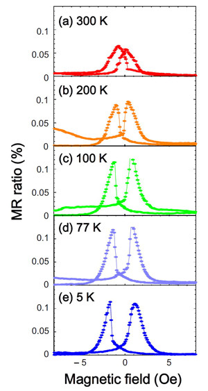
to 300 K. Whereas the magnetoresistance ratio of giant magnetoresistance
and tunnel magnetoresistance junctions monotonically increases with decreasing
temperature, that of our samples has the maximum value around 80 K and
decreases with decreasing temperature at lower than 80 K, which might be
due to an increase in the electrical conductivity mismatch between the
metallic Fe3Si layers and semiconducting FeSi2 interlayer in the low temperature
range .
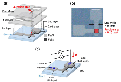
(a) Schematic diagram of deposition procedure of Fe3Si/FeSi2/Fe3Si junction,
(b) top view of the junction, and (c) electrical circuit for measuring
electrical resistance of the junction.
MR curves of Fe3Si/FeSi2/Fe3Si junction, measured at 300, 200, 100, 77,
and 5 K.
"Fabrication of Spin Valve Junctions Based on Fe3Si/FeSi2/Fe3Si Trilayered
films"
Fe3Si/FeSi2/Fe3Si trilayered junctions were prepared on Si(111) by facing
targets direct-current sputtering combined with a mask method, and spin
valve signals in current-perpendicular-to-plane (CPP) geometry was investigated
for the change of the magnetization alignment. The shape of magnetization
curves evidently exhibited that an antiparallel alignment is realized owing
to a difference in the coercive force between the top and bottom Fe3Si
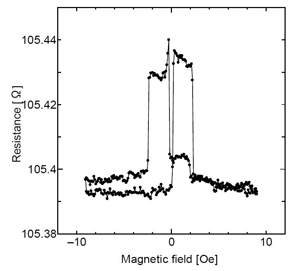
layers. The electrical resistance was alternately changed for the formation
of parallel and antiparallel alignments with the magnetic field. The spin
valve signals in the Fe3Si/FeSi2 trilayered junctions were experimentally
demonstrated.
(a) Preparation procedure of CPP trilayered junctions with masks, (b) top
view of CPP trilayered junction
MR curve of CPP trilayered film, measured at room temperature.
"Current-induced Magnetization Switching at Low Current Densities
in CPP Structural Fe3Si/FeSi2 Artificial Lattices"
Ken-ichiro Sakai, Yūta Noda, Takeshi Daio, Daiki Tsumagari, Aki Tominaga,
Kaoru Takeda, and Tsuyoshi Yoshitake
Jpn. J. Appl. Phys. Vol. 53, Issue 2S (2014) 02BC15.
Current-perpendicular-to-plane (CPP) junctions of Fe3Si/FeSi2 were fabricated
from Fe3Si/FeSi2 artificial lattice films, which were prepared by facing-target
direct-current sputtering, by employing a focused ion beam (FIB) technique.
CPP structurization was confirmed by scanning electron microscopy. The
CPP junctions, in which antiferromagnetic interlayer coupling is induced
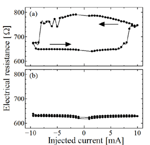
between the Fe3Si layers, exhibited a clear hysteresis loop in the electrical
resistance for current injection, which is probably due to current-induced
magnetization switching. The critical current density for it is approximately
3.3 ' 101A/cm2, which is at least four orders smaller than the values that
have ever been reported.
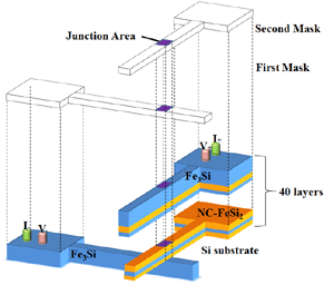
(a) Schematic of entire CPP junction and (b) planeview
SEM images of CPP junction and tungsten electrode deposited on Fe3Si
bottom layer.
Electrical resistance-injection current characteristics of CPP
junction.
"Temperature-dependent interlayer coupling in Fe3Si/FeSi2 artificial
lattices"
Ken-ichiro Sakai, Yuta Noda, Daiki Tsumagari, Hiroyuki Deguchi, Kaoru Takeda,
and Tsuyoshi Yoshitake
Phys. Status Solidi A 211, No. 2 (2014) 323–328.
Fe3Si/FeSi2 artificial lattices, wherein ferromagnetic (F)/antiferromagnetic
(AF) interlayer coupling between the Fe3Si layers were induced by controlling
the thickness of FeSi2 layers, were prepared on Si(111) substrates by facing
targets direct-current sputtering. The interlayer couplings were investigated
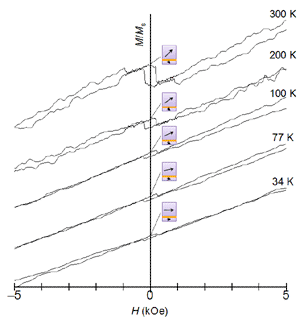
at different temperatures by measuring the magnetization curves. The AF
coupling at room temperature was gradually weakened with a decrease in
the temperature, and it finally became ferromagnetic or noncoupled at temperatures
lower than 77 K. We consider that the FeSi2 layers act as semiconductors
and their change in the electric state for the temperature induces the
interlayer coupling switching.
Change in magnetization curve of [Fe3Si(25 Å)/FeSi2(10 Å)]20 artificial
lattice for different temperature.
Change in interlayer coupling strength (J) with
temperature.
"Current-Induced Magnetization Switching in Fe3Si/FeSi2 Artificial Lattices"
Current-induced magnetization switching in Fe3Si/FeSi2 artificial lattices,
wherein ferromagnetic Fe3Si layers were antiferromagnetically coupled,
was studied in a current perpendicular to plane geometry. While the electrical
resistance-injected current (R-I) curve exhibited a clear hysteresis loop
under zero magnetic field, the hysteresis loop in the curve disappeared
under magnetic fields larger than the saturation magnetic field. This implies
that the interlayer coupling was altered from antiferromagnetic to ferromagnetic
by the current injection under zero magnetic field; on the other hand,
under the magnetic fields, the coupling was fixed to be ferromagnetic regardless
of the current injection.
Schematic diagram of deposition procedure of Fe3Si (100 Å)/[Fe3Si (25 Å)/FeSi2 (7.5 Å)]20/Fe3Si (100 Å) multilayered films.
Electrical resistance-injected current characteristics of Fe3Si (100 Å)/[Fe3Si (25 Å)/FeSi2 (7.5 Å)]20/Fe3Si (100 Å) multilayered films, measured under zero and 20 kOe magnetic
fields.
"Temperature-Dependent Current-Induced Magnetization Switching in
Fe3Si/FeSi2/Fe3Si trilayered films"
Jpn. J. Appl. Phys., Vol. 50, No. 8 (2011) 08JD06.
Fe3Si/FeSi2/Fe3Si trilayered films were grown on Si(111) substrates at
a substrate temperature of 300 ºC by facing targets direct-current sputtering,
and current-induced magnetization switching in current-perpendicular-to-plane
geometry was studied for the films wherein an antiferromagnetic interlayer
coupling perpendicular to the plane was probably formed at room temperature.
The appearance of a hysteresis loop in the electrical resistance-injection
current curve well coincided with that of a hysteresis loop in the magnetization
curve perpendicular to the plane. In addition, the hysteresis loop in the
electrical resistance-injection current curve disappeared under large magnetic
fields. The origin of the change in the electrical resistance for the injection
current might be attributable to the change in the interlayer coupling.
Magnetization curves of an Fe3Si/NC-FeSi2/Fe3Si trilayered film measured
under external magnetic fields (a) parallel and (b) perpendicular to the
plane.
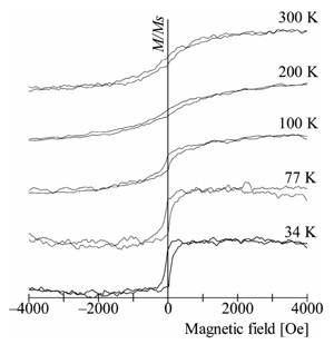
Magnetization curves perpendicular to the plane of an Fe3Si/NC-FeSi2/Fe3Si
trilayered film, measured at temperatures lower than 300 K.
"Enhanced interlayer coupling and magnetoresistance ratio in Fe3Si/FeSi2
superlattices"
[Fe3Si/FeSi2]20 superlattices were prepared on Si(111) at an elevated substrate
temperature of 300 ºC, and the magnetoresistance ratio and interlayer coupling
strengths were enhanced by approximately 100% and 34%, respectively, as
compared to those of superlattices deposited at room temperature. While
the elevated substrate temperature degraded the interface sharpness, the
crystalline orientation and the crystallinity of the Fe3Si layers were
apparently enhanced. The latters strongly influence on the interlayer coupling
and the magnetoresistance ratio. This implies that quantum well states
are tightly formed under the well-ordered crystalline planes, and the spin
diffusion lengths are improved due to the enhanced crystallinity.
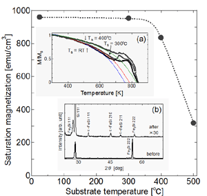
Change in Ms for Ts. The inset (a) shows the temperature dependence of
M/Ms of Fe3Si films deposited at various Ts values. The inset (b) shows
X-ray diffraction patterns of Fe3Si thin films deposited at RT before and
after the Tc measurement.
Cross-sectional TEM image of the [Fe3Si(25 Å)/FeSi2(60 Å)]20 superlattice.
(a) Bright field image, (b) dark field image obtained using a Fe3Si spot,
and (c) SAED pattern for the area including the substrate and the superlattice.
"Interlayer coupling in ferromagnetic epitaxial Fe3Si/FeSi2 superlattices"
Jpn. J. Appl. Phys. Part 1, Vol. 46, No. 12, 2007, pp. 7846–7848.
Fe3Si/FeSi2 superlattices were prepared on Si(111) at two deposition rates
by facing target direct-current sputtering. For the deposition rates of
2.0 nm/min for Fe3Si and 1.3 nm/min for FeSi2, the Fe3Si layers were nonoriented.
On the other hand, for half-deposition rates, the Fe3Si layers were epitaxially
grown not only on Si(111) but also up to the top layer across the FeSi2
layers. The antiferromagnetic interlayer coupling between the Fe3Si layers
was induced in the epitaxial superlattices, whereas it disappeared in the
nonepitaxial superlattices. The regular accumulation of highly oriented
Fe3Si layers is crucial for the interlayer coupling induction.
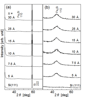
XRD patterns of [Fe3Si (25 Å)/FeSi2 (X Å)]20 superlattices, which were
deposited at deposition rate A, measured in (a) 2θ-θ mode and (b) 2θ mode
with fixed incidence angle of 4°.
XRD patterns of [Fe3Si (25 Å)/FeSi2 (X Å)]20 superlattices, which were
deposited at deposition rate B, measured in (a) 2q-q mode and (b) 2q mode
with fixed incidence angle of 4°. The inset shows typical f-scan patterns
of the superlattice with X = 7.5 Å, which was deposited at the deposition
rate B, and the Si(111) substrate.
"Interlayer coupling in ferromagnetic epitaxial Fe3Si/FeSi2 superlattices"
T. Yoshitake, T. Ogawa, D. Nakagauchi, D. Hara, M. Itakura, N. Kuwano,
Y. Tomokiyo, K. Takeda, T. Kajiwara, M. Ohashi, G. Oomi, and K. Nagayama
Appl. Phys. Lett. Vol. 89, 253110, 2006.
Ferromagnetic epitaxial B2-type Fe3Si/FeSi2 superlattices were prepared
on Si(111) at room temperature by facing targets direct-current sputtering.
The bilinear and biquadratic coupling constants J1 and J2 of the antiferromagnetically
coupled superlattice were comparable to those of the similar superlattices
using Fe layers although the saturation magnetization of Fe3Si is approximately
half as large as that of Fe. We believe that this is due to the formation
of a well-ordered quantum well in the spacers, which is mainly caused by
the regular accumulation of highly oriented Fe3Si layers.
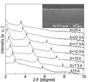
Low-angle X-ray diffraction patterns of the [Fe3Si(25 Å)/ FeSi2(X Å)]20
superlattices. The inset shows the cross-sectional TEM image of the [Fe3Si(25
Å)/FeSi2(17.5 Å)]20 superlattice.
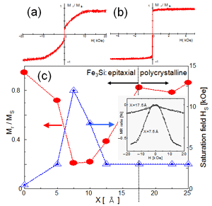
Typical magnetization curves of (a) antiferromagnetically and (b) ferromagnetically
or non-coupled superlattices (X = 7.5 Å and 17.5 Å) at room temperature.
(c) Change in Mr/Ms and Hs for the FeSi2 layer thickness X. The inset shows
typical MR curves of superlattices with X = 7.5 Å and 17.5 Å at room temperature.
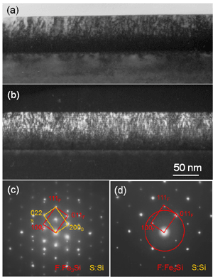
Cross-sectional TEM image of the [Fe3Si(25 Å)/FeSi2(7.5 Å)]20 superlattice.
(a) bright field image, (b) dark field image using a Fe3Si-011 spot. (c)
SAED pattern for the area including the substrate and the film, (d) SAED
pattern for the film.